WANG Xinhua, WANG Qizhi, TU Chengyuan, CHEN Yingchun. High-frequency Isolation Drive Circuit of Exciting Source for Electromagnetic Ultrasonic Phased Array[J]. Journal of Beijing University of Technology, 2017, 43(6): 826-832. DOI: 10.11936/bjutxb2016060031
Citation:
WANG Xinhua, WANG Qizhi, TU Chengyuan, CHEN Yingchun. High-frequency Isolation Drive Circuit of Exciting Source for Electromagnetic Ultrasonic Phased Array[J]. Journal of Beijing University of Technology, 2017, 43(6): 826-832. DOI: 10.11936/bjutxb2016060031
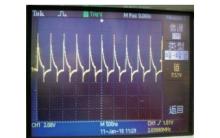
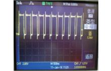
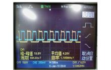
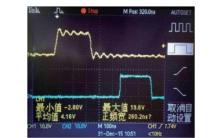
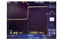
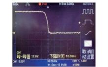
In order to further improve the work efficiency of exciting source for electromagnetic ultrasonic phased array, a method of gate drive circuit design of high frequency isolation for exciting source of electromagnetic ultrasonic phased array was presented in this paper based on half bridge topology structure. Through analyzing the process of turn-on and turn-off loss of MOSFET based on the simplified model structure of MOSFET, satisfied conditions of drive circuit with high frequency isolation were put forward and the reference potential was converted by using fiber optic components isolated pulse signal and DC-DC power supply. The high frequency “floating gate” problem of drive circuit was solved effectively, and the dead-time adjustable circuit was designed by combining the RC differential circuit with Schmitt inverter. The experimental results show that the design of drive circuit can output drive signal in which the frequency is 1.1MHz, the dead-time is 0.32μs, the voltage amplitude is 18.8V, and the duty ratio is 26%. The drive circuit reduces power loss of power switch tube effectively in the practical application of driving MOSFET.
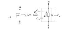
在MOSFET的简化模型中,漏极、源极、栅极之间存在3个寄生电容:
C
GD、
C
GS、
C
DS,三者间的关系为
C
GD=C
rss(1)
C
GS=C
iss-Crss(2)
C
DS=C
oss-Crss(3)
式中:
Ciss为输入电容;
Coss为输出电容;
Crss为反向传输电容
.
C
GD、
C
GS、
C
DS之间的关系影响着MOSFET各极间的电荷量和开通关断过程
. 如
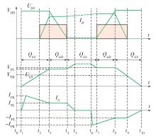
图2所示,MOSFET开通过程中,
t1~t2是其开通延时阶段,栅源极间电容
C
GS开始充电,当上升到开启阀值电压
UTH,时间参数为(
R
G+R
DS(on))
Ciss,
U
DS保持外加直流电压
V
DD不变,漏极没有电流流过(
I
D=
0),栅极电流
I
G最高达到
IPK;
t2~t3阶段,
U
GS电压从
VTH按指数规律增到米勒平台电压
VPL,
I
D开始缓慢增加,到
t3时刻,
I
D上升到最大值,
U
DS=V
DD保持不变,电荷量为
Q
GS;
t3~t4阶段,漏极电流保持恒定的最大电流值
I
D,漏源电压
U
DS开始下降,反向传输电容(
Crss)
C
GD的米勒效应使得
U
GS保持不变,MOSFET管固有的转移特性使得栅极电压与漏极电流维持比例关系,栅源极间的电容
C
GS不再流过电流,驱动的电流全部流过米勒电容,其电荷量为
Q
GD,栅极电流
I
G保持在平台电流
IPL值不变;
t4~t5阶段,栅极处于过驱动状态,但驱动部分仍然在消耗能量,过了米勒平台后,MOSFET已经完全导通,栅极电压和漏极电流不再受转移特性的束缚,继续增大,直至驱动电压,此时,栅极电流
I
G用于给
C
GS、
C
GD充电
.
MOSFET的关断过程为
图2中的
t6~t10,正好与开通过程相反,经过一段的关断延时和栅极即间电容
C
GS开始放电后,进入一段米勒平台,栅源电压
U
GS开始上升,MOSFET管逐渐关断,直至漏极电流
I
D=
0,此时开关管彻底关断
.
由
图2可知,MOSFET的功率损耗主要发生在
U
DS和
I
D交叉重叠区域
. 3个极间电容(
C
GD、
C
GS、
C
DS)在每次开关转换中需要充电、放电以达到新的电压值与开关状态改变相对应,所以交叠会持续一段时间
. 总之,电容值越大,充电时间就越长,交叠时间就会越长,结果导致交叠损耗就越大
.
开通过程中产生的开关损耗为
Ploss(on)=fsV
DDI
D(
t4-t2)(4)
关断过程中产生的开关损耗为
Ploss(off)=fsV
DDI
D(
t9-t7)(5)
从式(4)(5)可知,开通和关断损耗决定因素是电流和电压各自完成转换所需的时间(
t4-t2)和(
t9-t7),转换的快慢是随着驱动电阻和极间寄生电容乘积大小而变化的
. 当然,在工艺方面,通过改良MOSFET自身的寄生电容和饱和导通后的导通电阻
R
DS(on),降低开关功率损耗
. 但是,MOSFET在实际应用过程中,只能通过对其外部驱动电路结构的精准有效设计,才能弥补MOSFET自身工艺制造方面的缺陷,降低开关管在高速工作状态的功率损耗,有效地提高功率放大电路输出功率
.
JIN SJ,YANG XX,CHEN SL,et al.Development and application of ultrasonic phased array inspection technology[J].Journal of Electronic Measurement and Instrumentation,2014,28(9):925-934. (in Chinese)
[2]
YAMADAH,YANOY,UDAGAWAT.Development of the phased array system for angle beam testing[J]. Nippon Steel Technical Report,2004(98):28-32.
FUJITAH,AKAGIH,SHIVOHARAS.A 2-MHz, 6-kVA voltage-source inverter using low-profile MOSFET modules for low-temperature plasma generators[J].IEEE Transactions on Power Electronics,1999,14(6):1014-1020.
WANG SJ,ZHAO ZX,ZHAI GF.Detection system about train-wheels cracks based on electronic ultrasonic technology[J]. Instrument Technique and Sensor,2005(11):27-29. (in Chinese)
LI ZY,CHENP,WANGS.Exciting source research of electromagnetic ultrasonic transducer based on RLC oscillating circuit[J].Journal of Sichuan Ordnance,2009,30(4):83-85. (in Chinese)
LIP,HUANG SL,WANGK,et al.Development of a pulse exciting source for electromagnetic ultrasonic detection[J].Electrical Measurement & Instrumentation,2012,554(49):76-83. (in Chinese)
[8]
IRWIN LN.High-performance lossless RF fiber optic linkC]∥IEEE International Symposium on Phased Array Systems and Technology. Dana Point, California: IEEE
2000375378
IRWIN LN.High-performance lossless RF fiber optic link[C]∥IEEE International Symposium on Phased Array Systems and Technology. Dana Point, California: IEEE,2000:375-378.
YAN HS,ZHOU WS,WANG PQ,et al.Design of power MOSFET driver circuit for high frequency induction heating[J].Supply Power Electronics,2007,41(4):91-99. (in Chinese)
[11]
JEMISONL WDWEY TAPAOLELLAA.A new optoelectronic oscillator topology based on a class e analog fiber optic linkC]∥2010 IEEE MTT-S International Microwave Symposium. Anaheim, California: IEEE
2010736739
JEMISONL WD,WEY TA,PAOLELLAA.A new optoelectronic oscillator topology based on a class e analog fiber optic link[C]∥2010 IEEE MTT-S International Microwave Symposium. Anaheim, California: IEEE,2010:736-739.

 下载: 导出CSV